In this article we are design verilog code for cdc solutions, so Here is a list of some of the common clock domain crossing (CDC) solutions:
- Synchronizer
- Two-Flop Synchronizer
- Gray Code Encoding
- FIFO
- Handshaking Protocol
- Dual-Data Rate (DDR) Interface
- Asynchronous FIFO
These are just a few examples of CDC solutions, and there may be other solutions that are specific to a given design. It is important to carefully consider the options and choose the best solution for a given system.
1] 2 flip-flop synchronizer
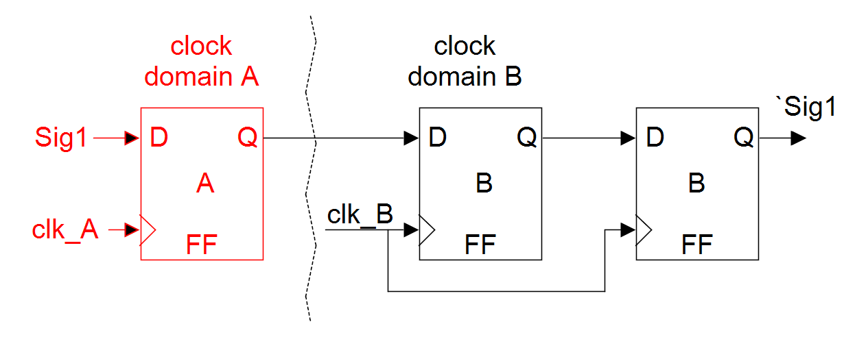
This is a simple 2ff synchronizer, where data is sample by one clock domain A and data is capture by another clock domain B. I t is useful for single bit transfer from domain A to B. It is suitable situation, where clock A is at slow speed and clock B at higher speed B > A. If this condition not there then data loss will be there.
module two_ff_synch( input clk1, clk2, reset, sig1, output osig1);

reg q1,q2,q3;

//------- clock domain 1

always @ ( posedge clk1 ,negedge reset)

if (~reset)

q1 <= 1'b0;

else

q1 <= sig1;

always @ ( posedge clk2 ,negedge reset)

if (~reset) begin

q2 <= 1'b0;

q3 <= 1'b0;

end else begin

q2 <= q1;

q3 <= q2;

end

assign osig1 = q3;

endmodule
and test bench for it as
`timescale 1ns / 10ps

module tb_two_ff_synch();

reg clk1,clk2,reset,sig1;

wire osig1;

always #300 clk1 = ~clk1;

always #50 clk2 = ~clk2;

initial

begin

clk1 = 1'b0;

clk2 = 1'b0;

reset = 1'b0;

sig1 = 1'b0;

#100;

reset = 1'b1;

repeat (3)

begin

#300;

sig1 = 1'b1;

#600;

sig1 = 1'b0;

#600;

end

#300;

// $finish;

end

two_ff_synch inst (

.clk1(clk1),

.clk2(clk2),

.reset(reset),

.sig1(sig1),

.osig1(osig1));

endmodule
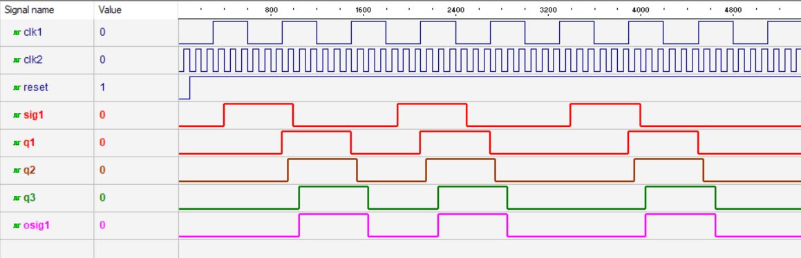
case 1 wave form clk1 < clk2 its looks ok
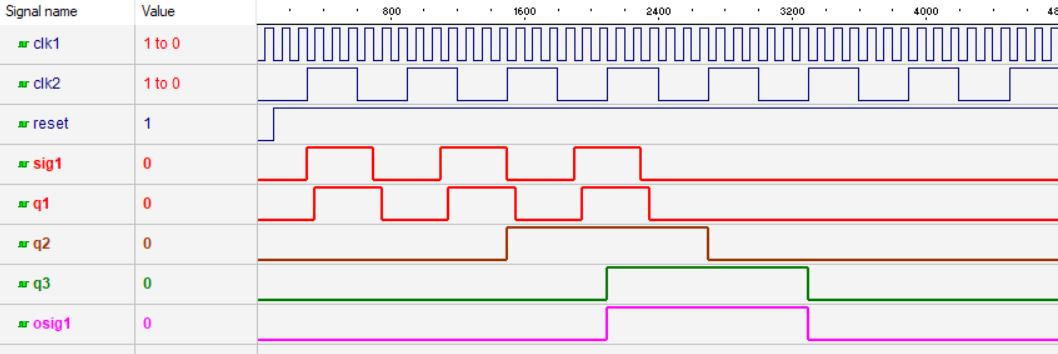
 case 1 wave form clk1 > clk2 it is having issue, data loss
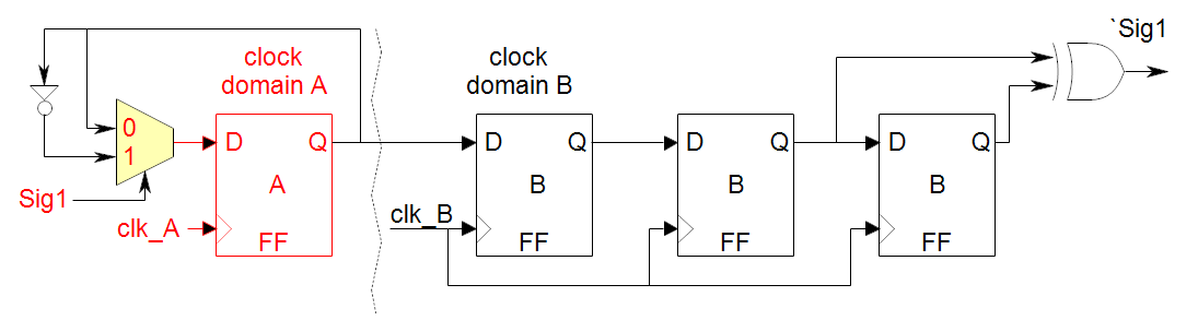
2] Toggle synchronizer
Toggle synchronizer is used to synchronize a pulse generating in source clock domain to destination clock domain. A pulse cannot be synchronized directly using 2 FF synchronizer. While synchronizing from fast clock domain to slow clock domain using 2 FF synchronizer, the pulse can be skipped which can cause the loss of pulse detection & hence subsequent circuit which depends upon it, may not function properly.
code for toggle synchronizer
module toggle_ff_synch( input clk1, clk2, reset, sig1, output osig1);

reg q1,q2,q3,q4;

//------- clock domain 1

wire mux_op;

assign mux_op = sig1? ~q1: q1 ;

always @ ( posedge clk1 ,negedge reset)

if (~reset)

q1 <= 1'b0;

else

q1 <= mux_op;

//------- clock domain 2

always @ ( posedge clk2 ,negedge reset)

if (~reset) begin

q2  <= 1'b0;

q3  <= 1'b0;

q4  <= 1'b0;

end else begin

q2  <= q1;

q3  <= q2;

q4  <= q3;

end

assign osig1 = q3 ^ q4;

endmodule
test bench for toggle synchronizer
`timescale 1ns / 10ps

module tb_toggle_ff_synch();

reg clk1,clk2,reset,sig1;

wire osig1;

always #300 clk1 = ~clk1;

always #50 clk2 = ~clk2;

initial

begin

clk1 = 1'b0;

clk2 = 1'b0;

reset = 1'b0;

sig1 = 1'b0;

#600;

reset = 1'b1;

repeat (3)

begin

sig1 = 1'b1;

#800;

sig1 = 1'b0;

#2200;

end

#300;

// $finish;

end

toggle_ff_synch inst (

.clk1(clk1),

.clk2(clk2),

.reset(reset),

.sig1(sig1),

.osig1(osig1));

endmodule
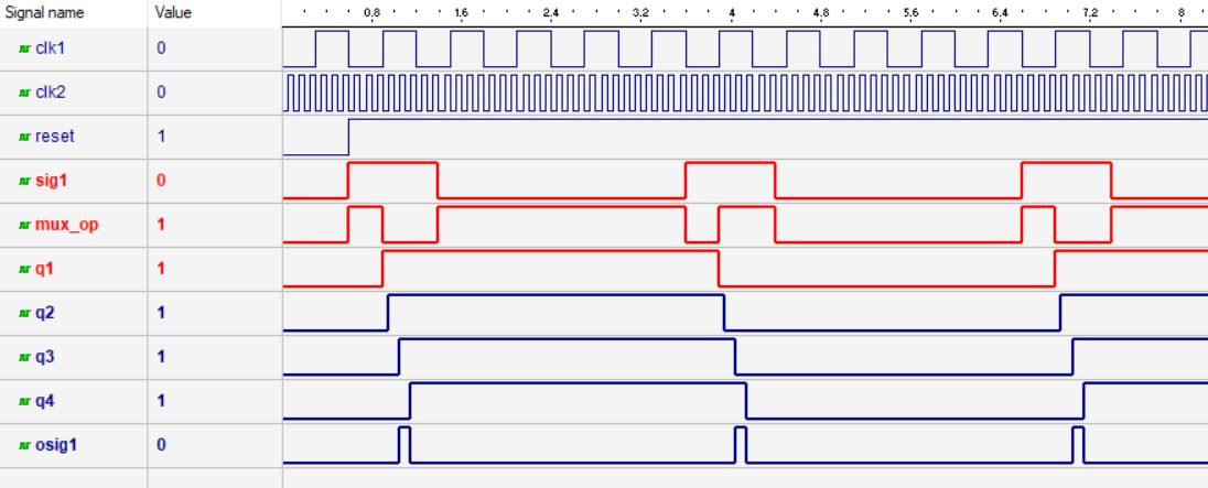
Personally, not satisfy with the result from this synchronizer
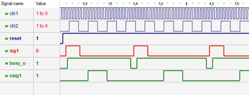
3] Handshake based pulse synchronizer
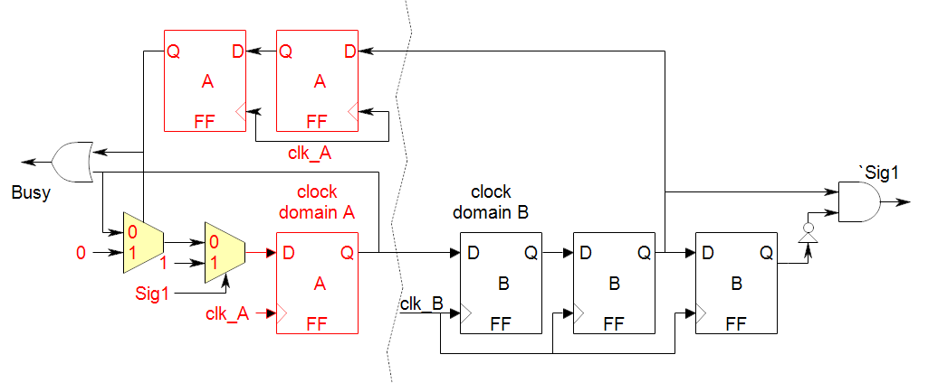
In handshake based pulse synchronizer, as shown in diagram, synchronization of a pulse generated into source clock domain is guaranteed into destination clock domain by providing an acknowledgement. There is one restriction in pulse synchronizer that back to back (one clock gap) pulses cannot be handled. To make sure the next generated pulse in source clock domain gets definitely transferred and synchronized in the destination clock domain, the handshake based pulse synchronizer generates a “Busy” signal by ORing A1 and A3 flip-flop outputs. Thus the logic generating the pulse shall not generate another pulse till the busy signal is asserted.
The code
`timescale 1ns / 10ps

module HS_pulse_synch(clk1,clk2,reset,sig1,osig1,busy_o);

input  clk1,clk2,reset,sig1;

output osig1,busy_o;

wire dfin;

reg qA,qA_fb0,qA_fb1,qB0,qB1,qB2;

assign dfin = sig1? 1'b1:(qA_fb1? 1'b0:qA);

always @(posedge clk1,negedge reset)

begin

if (~reset)

qA <= 1'b0;

else

qA <= dfin;

end

always @(posedge clk2,negedge reset)

begin

if (~reset) begin

qB0 <= 1'b0;

qB1 <= 1'b0;

qB2 <= 1'b0;

end

else begin

qB0 <= qA;

qB1 <= qB0;

qB2 <= qB1;

end

end

assign osig1 = ~qB2 & qB1 ;

always @(posedge clk1,negedge reset)

begin

if (~reset)

begin

qA_fb0 <= 1'b0;

qA_fb1 <= 1'b0;

end

else

begin

qA_fb0 <= qB1;

qA_fb1 <= qA_fb0;

end

end

assign busy_o = qA | qA_fb1 ;

endmodule
The test bench
`timescale 1ns / 10ps

module tb_HS_pulse_synch();

reg clk1,clk2,reset,sig1;

wire osig1,busy_o;

always #50  clk1 = ~clk1;

always #300 clk2 = ~clk2;

initial

begin

clk1 = 1'b0;

clk2 = 1'b0;

reset  = 1'b0;

sig1    = 1'b0;

#100;

reset  = 1'b1;

repeat (3)

begin

wait(~busy_o);

#100;

sig1  = 1'b1;

#450;

sig1  = 1'b0;

#100;

end

#1000;

$finish;

end

HS_pulse_synch inst (

.clk1(clk1),

.clk2(clk2),

.reset(reset),

.sig1(sig1),

.osig1(osig1),

.busy_o(busy_o));

endmodule
All the above methods is for single bit transfer, but When multi bit signals are synchronized with let say by 2 flip flop synchronizer, each bit is synchronized using separate 2-FF synchronizer. Metastability can cause a flip flop to settle down either to a true value or a false value. So output of every synchronizer may not settle to correct value at same clock. This causes data incoherency.
For multibit transfer solutions are
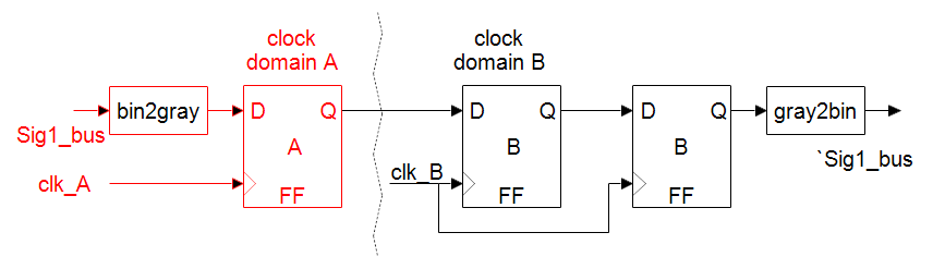
1] Gray encoder
In order to synchronize multi bit signal using 2 flip flop synchronizer method, only a single bit change must be guaranteed at a particular clock cycle. This can be achieved by gray encoding.
 2] Recirculation mux synchronization
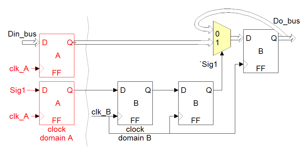 For isolated data and where multiple bits can transit at the same time, Recirculation mux synchronization technique shown in diagram is used. In order to synchronize data, a control pulse[Sig1] is generated in source clock domain when data is available at source flop. Control Pulse[Sig1] is then synchronized using 2 flip flop synchronizer or pulse synchronizer (Toggle or Handshake) depending on clock ratio between source and destination domain. Synchronized control pulse[`Sig1] is used to sample the data on the bus in destination domain. Data should be stable until it is sampled in destination clock domain.
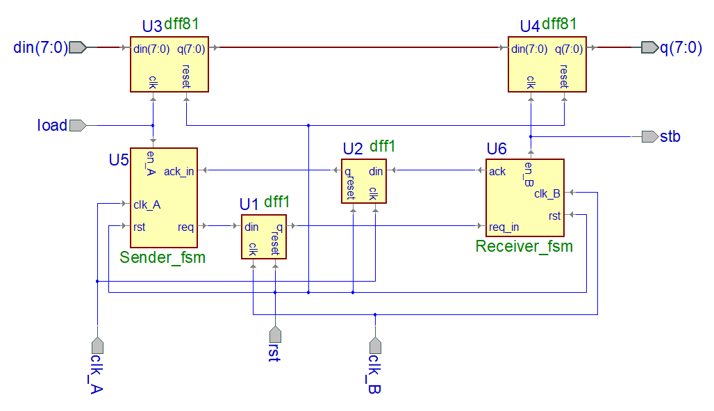
3] Handshake synchronization
In this synchronization scheme request and acknowledge mechanism is used to guarantee the sampling of correct data into destination clock domain irrespective of clock ratio between source clock and destination clock. This technique is mainly used to synchronize vector signal which is not changing continuously or very frequently. As shown in diagram, data should remain stable on the bus until synchronized Acknowledge signal (A2-q) is received from destination side and it (A2-q) goes low. Diagram shows this implementation also shows timing for handshake synchronizer.
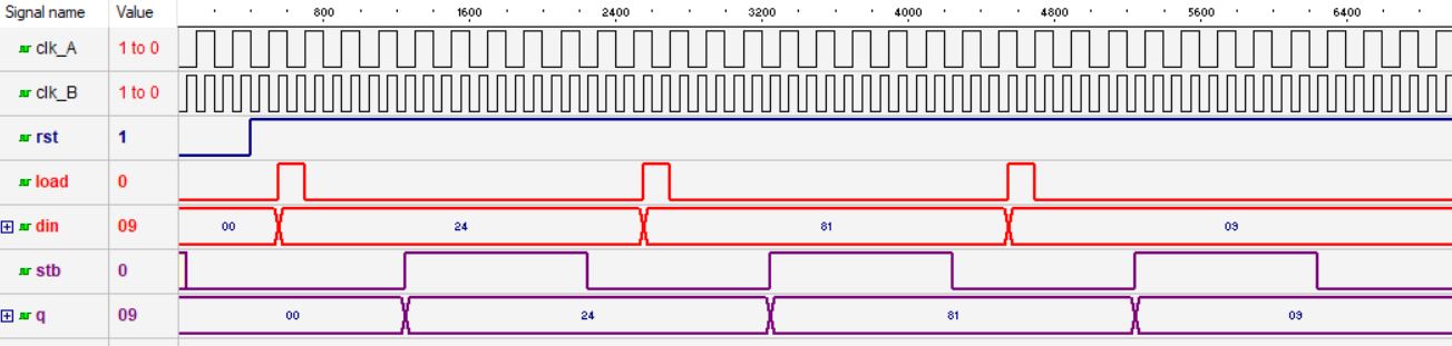
 when clk_A < clk_B
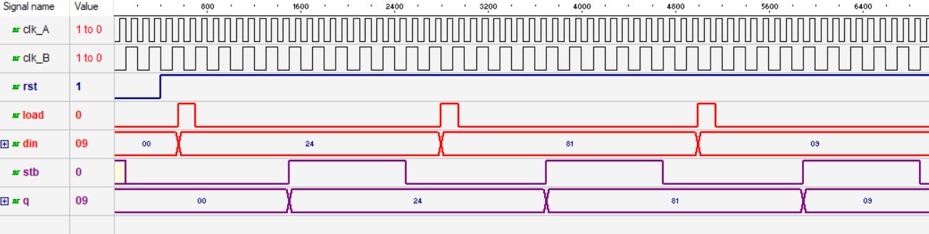
 when clk_A > clk_B
codes are here
dff1 module
module dff1 (din,clk,reset,q);

input din, clk, reset ;

output q;

reg t[1:0];

always @ ( posedge clk, negedge reset)

if (~reset) begin

t[0] <= 1'b0;

t[1] <= 1'b0;

end  else begin

t[0] <= din;

t[1] <= t[0];

end

assign q = t[1];

endmodule
dff81 module
module dff81 (din,clk,reset,q );

input   [7:0] din;

input clk, reset ;

output  [7:0] q;

reg [7:0] t;

always @ ( posedge clk, negedge reset)

if (~reset) begin

t <= 8'b0000_0000;

end  else begin

t <= din ;

end

assign q = t ;

endmodule
Sender_fsm
`timescale 1ns / 1ps

module Sender_fsm (ack_in, clk_A, en_A, req, rst);

input      	ack_in;

input      	clk_A;

input      	en_A;

input      	rst;

output     	req;

wire        ack_in;

wire        clk_A;

wire        en_A;

reg         req, next_req;

wire        rst;

// BINARY ENCODED state machine: Sreg0

// State codes definitions:

`define S1 2'b00

`define S2 2'b01

`define S3 2'b10

reg [1:0] CurrState_Sreg0;

reg [1:0] NextState_Sreg0;

// Diagram actions (continuous assignments allowed only: assign ...)

// Diagram ACTION

//--------------------------------------------------------------------

// Machine: Sreg0

//--------------------------------------------------------------------

//----------------------------------

// Next State Logic (combinatorial)

//----------------------------------

always @ (ack_in or en_A or req or CurrState_Sreg0)

begin : Sreg0_NextState

NextState_Sreg0 <= CurrState_Sreg0;

// Set default values for outputs and signals

next_req = req;

case (CurrState_Sreg0) // synopsys parallel_case full_case

`S1:

begin

next_req = 1'b0;

if (en_A==1'b1)

NextState_Sreg0 <= `S2;

else

NextState_Sreg0 <= `S1;

end

`S2:

begin

next_req = 1'b1;

if (en_A==1'b0)

NextState_Sreg0 <= `S3;

else

NextState_Sreg0 <= `S2;

end

`S3:

begin

next_req = 1'b1;

if (ack_in==1'b1)

NextState_Sreg0 <= `S1;

else

NextState_Sreg0 <= `S3;

end

endcase

end

//----------------------------------

// Current State Logic (sequential)

//----------------------------------

always @ (posedge clk_A)

begin : Sreg0_CurrentState

if (rst==0)

CurrState_Sreg0 <= `S1;

else

CurrState_Sreg0 <= NextState_Sreg0;

end

//----------------------------------

// Registered outputs logic

//----------------------------------

always @ (posedge clk_A)

begin : Sreg0_RegOutput

if (rst==0)

begin

req <= 1'b0;

end

else

begin

req <= next_req;

end

end

endmodule
Receiver_fsm
`timescale 1ns / 1ps

module Receiver_fsm (ack, clk_B, en_B, req_in, rst);

input      	clk_B;

input      	req_in;

input      	rst;

output     	ack;

output     	en_B;

reg         ack, next_ack;

wire        clk_B;

reg         en_B, next_en_B;

wire        req_in;

wire        rst;

// BINARY ENCODED state machine: Sreg0

// State codes definitions:

`define S1 1'b0

`define S2 1'b1

reg CurrState_Sreg0;

reg NextState_Sreg0;

// Diagram actions (continuous assignments allowed only: assign ...)

// Diagram ACTION

//--------------------------------------------------------------------

// Machine: Sreg0

//--------------------------------------------------------------------

//----------------------------------

// Next State Logic (combinatorial)

//----------------------------------

always @ (ack or en_B or req_in or CurrState_Sreg0)

begin : Sreg0_NextState

NextState_Sreg0 <= CurrState_Sreg0;

// Set default values for outputs and signals

next_ack = ack;

next_en_B = en_B;

case (CurrState_Sreg0) // synopsys parallel_case full_case

`S1:

begin

next_ack = 1'b0;

next_en_B = 1'b0;

if (req_in==1'b1)

NextState_Sreg0 <= `S2;

else

NextState_Sreg0 <= `S1;

end

`S2:

begin

next_ack = 1'b1;

next_en_B = 1'b1;

if (req_in==1'b0)

NextState_Sreg0 <= `S1;

else

NextState_Sreg0 <= `S2;

end

endcase

end

//----------------------------------

// Current State Logic (sequential)

//----------------------------------

always @ (posedge clk_B)

begin : Sreg0_CurrentState

if (rst==0)

CurrState_Sreg0 <= `S1;

else

CurrState_Sreg0 <= NextState_Sreg0;

end

//----------------------------------

// Registered outputs logic

//----------------------------------

always @ (posedge clk_B)

begin : Sreg0_RegOutput

if (rst==0)

begin

ack <= 1'b0;

en_B <= 1'b0;

end

else

begin

ack <= next_ack;

en_B <= next_en_B;

end

end

endmodule
Top module HS_synch1
`timescale 1ps / 1ps

module HS_synch1 (clk_A,clk_B,load,rst,din,stb,q) ;

// ------------ Port declarations --------- //

input clk_A;

wire clk_A;

input clk_B;

wire clk_B;

input load;

wire load;

input rst;

wire rst;

input [7:0] din;

wire [7:0] din;

output stb;

wire stb;

output [7:0] q;

wire [7:0] q;

// ----------- Signal declarations -------- //

wire NET113;

wire NET132;

wire NET75;

wire NET85;

wire [7:0] BUS594;

// -------- Component instantiations -------//

dff1 U1

(

.clk(clk_B),

.din(NET75),

.q(NET132),

.reset(rst)

);

dff1 U2

(

.clk(clk_A),

.din(NET113),

.q(NET85),

.reset(rst)

);

dff81 U3

(

.clk(load),

.din(din),

.q(BUS594),

.reset(rst)

);

dff81 U4

(

.clk(stb),

.din(BUS594),

.q(q),

.reset(rst)

);

Sender_fsm U5

(

.ack_in(NET85),

.clk_A(clk_A),

.en_A(load),

.req(NET75),

.rst(rst)

);

Receiver_fsm U6

(

.ack(NET113),

.clk_B(clk_B),

.en_B(stb),

.req_in(NET132),

.rst(rst)

);

endmodule
Test bench for HS_synch1
`timescale 1ns / 10ps

module tb_HS_synch1();

reg clk_A,clk_B,rst,load;

reg  [7:0] din;

wire [7:0] q;

wire stb;

always #50  clk_A = ~clk_A;

always #100 clk_B = ~clk_B;

initial

begin

clk_A   = 1'b0;

clk_B   = 1'b0;

rst     = 1'b0;

load    = 1'b0;

din     = 8'd0;

#400;

rst  = 1'b1;

repeat (3)

begin

#150;

load  = 1'b1;

din   = $random;

#150;

load  = 1'b0;

wait(stb);

wait(~stb);

//load  = 1'b0;

#150;

end

#1000;

//$finish;

end

HS_synch1 inst (

.clk_A(clk_A),

.clk_B(clk_B),

.rst(rst),

.load(load),

.stb(stb),

.din(din),

.q(q));

endmodule
External Link https://www.edn.com/synchronizer-techniques-for-multi-clock-domain-socs-fpgas/?unapproved=29933&moderation-hash=e81845cd523fde33e9140793a5b9c1ed#comment-29933
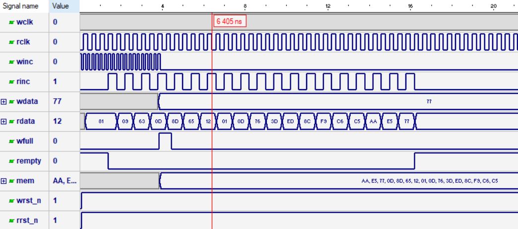
4] Asynchronous FIFO synchronization
FIFO is best way to synchronize continuously changing vector data between two asynchronous clock domains. Asynchronous FIFO synchronizer offers solution for transferring vector signal across clock domain without risking metastability and coherency problems. In Asynchronous FIFO design, FIFO provides full synchronization independent of clock frequency. As shown in diagram , read and write pointers are synchronized to write and read clock domains respectively after performing binary to gray conversion.
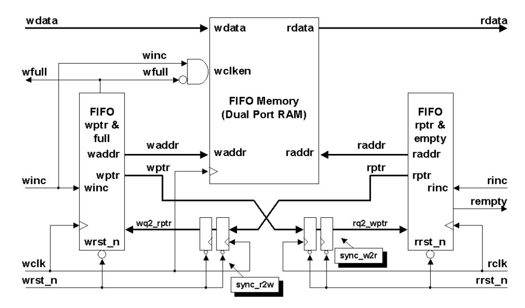 [source for fifo: Sunburst Design]

Comments are welcome, let me know any farther code modification / suggestion