Hi, after many projects on the power line communication for AC and DC line, There are many power line modems chips are there which convert the bit 1/0 into FSK, like for 1-1200hz, for 0-2200hz which then superimpose on to the power line.
While working with DC power line communication called HART communication for the ds8500 HART chip, I came across it is very tough to make it alone with 4-20ma loop circuit arrangement. Not found well define application circuit around it.
Well most important part is the system setup with the power supply arrangement.
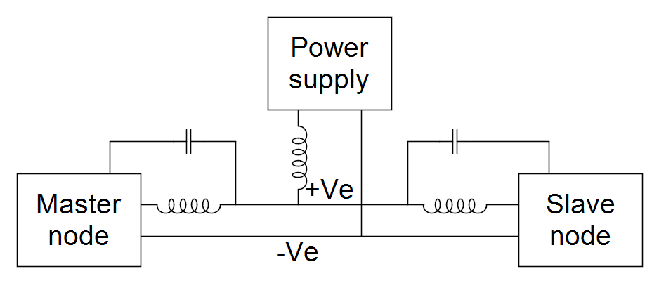 A two node and power supply is shown in the block diagram. As it seen from the diagram there is inductor L is place which will block the any high frequency entering to the power supply of individual node if not place the inside regulator or filtering capacitor will remove any signal on DC line. so logically this L make line float for signal which can be superimpose on or take it to from for receive using coupling capacitor. generally L of value 2mH and 2.2uF capacitor can be used for such setup.
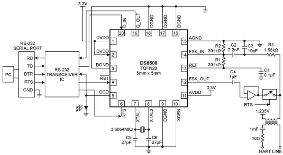
The application diagram of DS8500 from datasheet link
https://www.analog.com/media/en/technical-documentation/tech-articles/introduction-to-the-ds8500-hart-modem.pdf
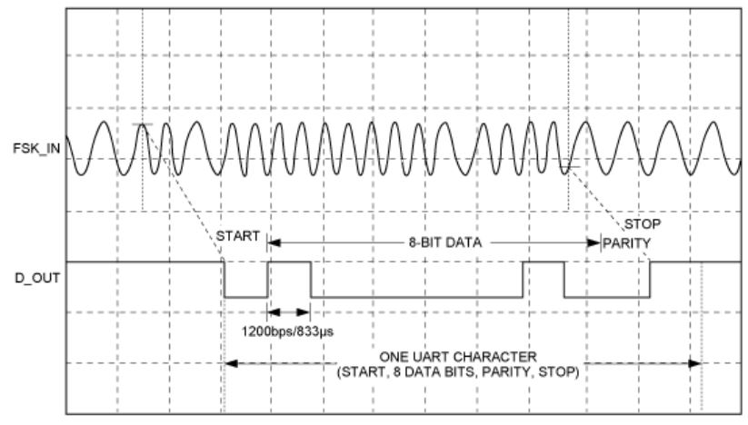
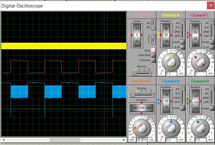
Modulation waveform
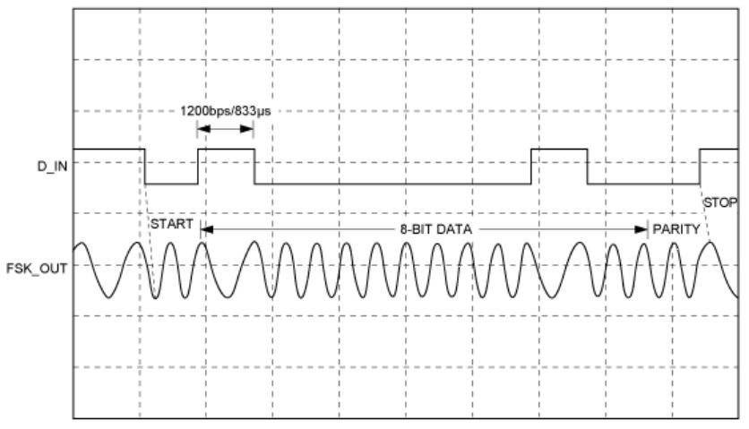
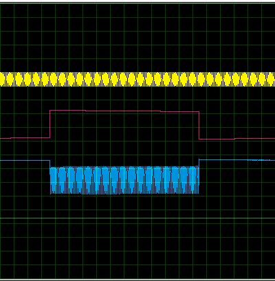
Demodulation waveform
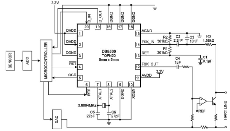
HART slave using DS8500 circuitry and the top-level blocks necessary for an intelligent process transmitter. A temperature process transmitter serves as an example for this circuit. The sensor on the process transmitter measures the system temperature in current or voltage and then passes the data to
the ADC. The ADC, in turn, converts these analog signals to digital equivalents for the microcontroller to process. The microcontroller provides remote memory along with computation power. The microcontroller typically hosts the HART stack and is responsible for the protocol implementation; it also processes the digital data from the HART modem. Microcontroller capabilities can also be used for sensor calibration, linearization and signal conditioning. The DAC is primarily responsible for driving the current loop. On the master side, the DS8500 can be part of the master modem that resides either on the central control unit or the handheld HART communicator.
shows the master-side configuration. In this case, the DS8500 communicates to the PC through an RS-232 serial port. The HART protocol is usually supported by software that can be installed on the computer.
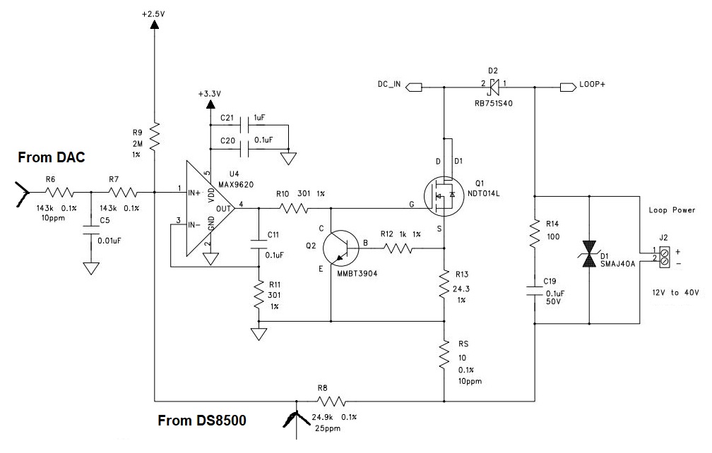
The more detail circuit found from some where from its evaluation circuit details,
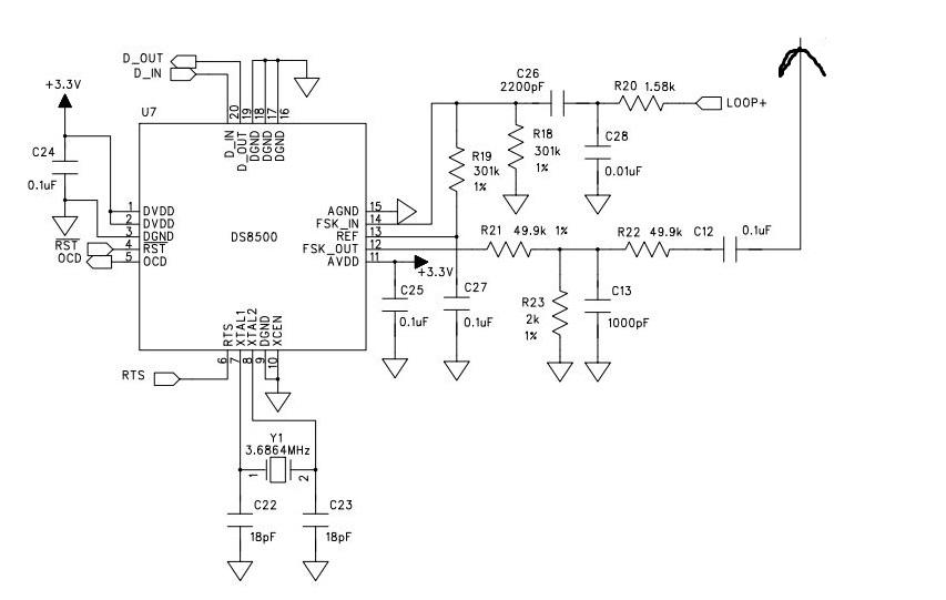
And the DS8500 circuit design as below but it is part of the complete design, here i only given the ds related circuit.
I recommend to use amplifier to boot the fsk out signal from ds8500, which i found in different application note else isolation transform can be used for such amplification with proper turn ratio.
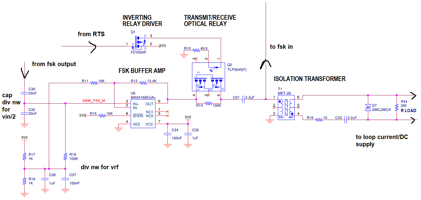
The amplifier in simple form
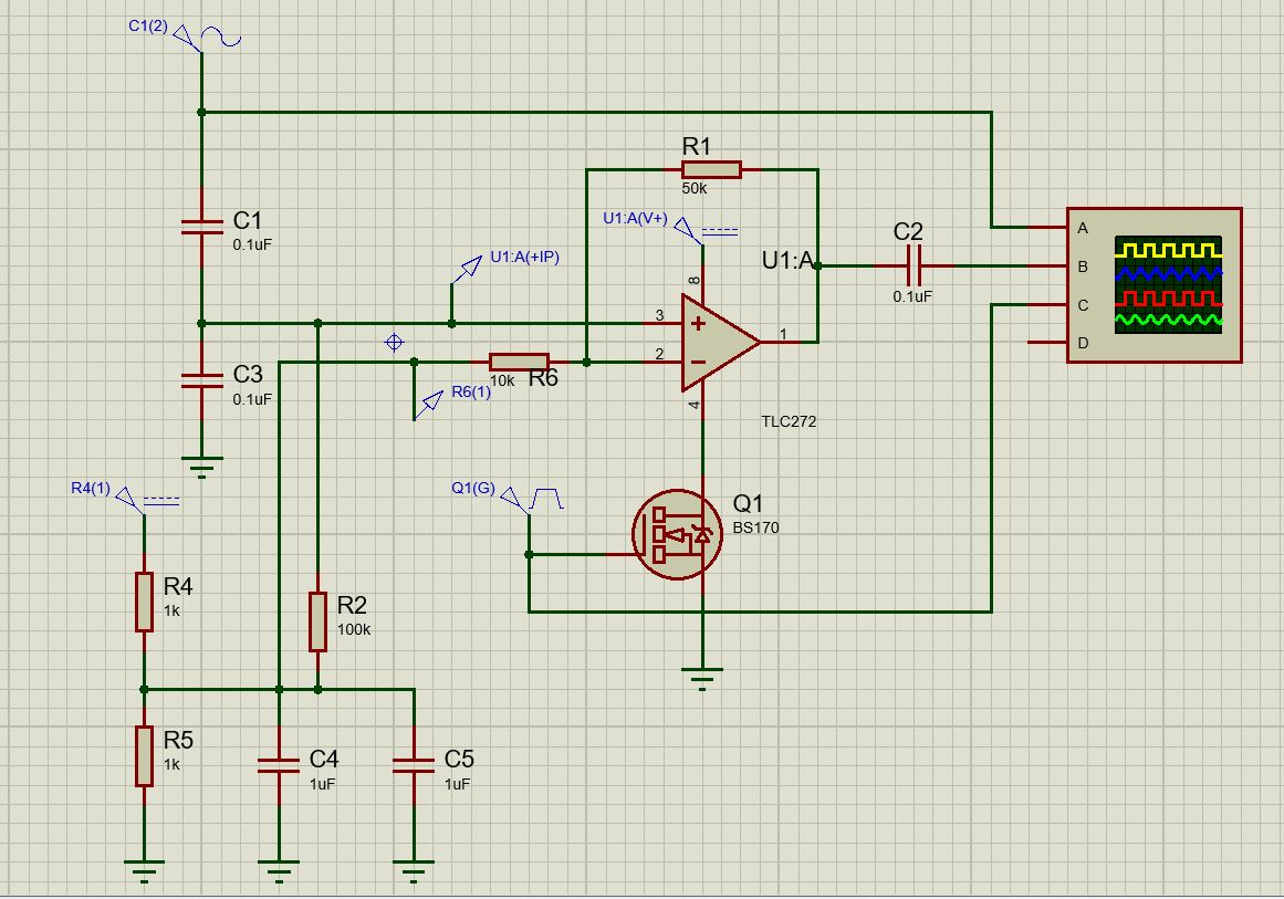
mosfet is use for the disable the unnecessary signals during ideal time.
Now for AC the, had worded with TDA5051 PLC chip, sharing some information about it, you can go thro its datasheet in details while working on it.
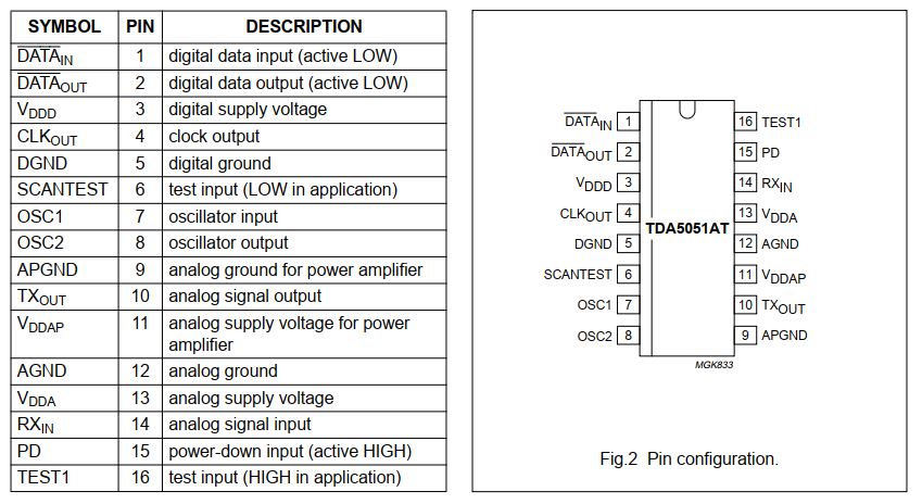
The pin description, DATA in out and TXout and RXin PD pins used for interface with the MC or host controller.
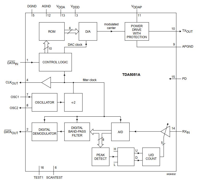 For every PLC communication AC and DC data sending concept is same, convert the bit 1/0 into its corresponding assigned frequency [FSK] f1/f2 and at the receiver side do the revers to get the bit 1/0. from the block diagram you can see the process data input is placed at DATAin pin which then converted to FSK at the TXout using ROM and dac circuit. Similar at the receiver side analog signal converted in to digital using ADC, filter the signal using digital filter then demodulate it.
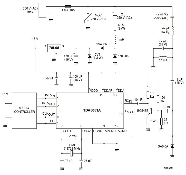
There are two application circuit on the bases of isolation [1] non-isolated PLC [2] isolated PLC design.
1] Non isolated PLC circuit is shown below,

1.1] Non-isolated PLC circuit is shown below,
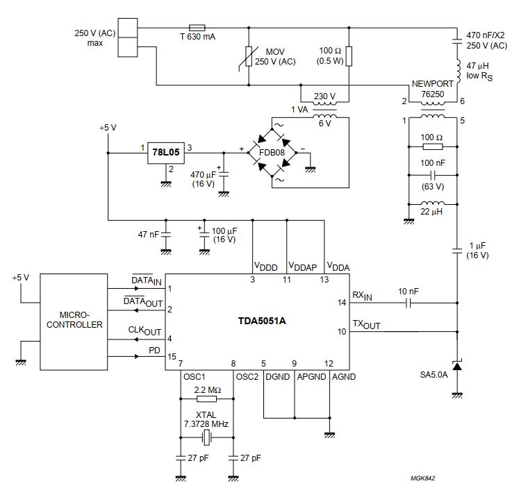
 2] Isolated PLC circuit is shown below,
1.functional Description
Both transmission and reception stages are controlled either by the master clock of the micro-controller, or by the on-chip reference oscillator connected to a crystal. This holds for the accuracy of the transmission carrier and the exact trimming of the digital filter, thus making the performance totally independent of application disturbances such as component spread, temperature, supply drift and so on. The interface with the power network is made by means of a LC network . The device includes a power output stage able to feed a 120 dBmV (RMS) signal on a typical 30 W load. To reduce power consumption, the IC is disabled by a power-down input (pin PD): in this mode, the on-chip oscillator remains active and the clock continues to be supplied at pin CLKOUT. For low-power operation in reception mode, this pin can be dynamically controlled by the micro controller (see Section “Power-down mode”). When the circuit is connected to an external clock generator , the clock signal must be applied at pin OSC1 (pin 7); OSC2 (pin 8) must be left open. Use of the on-chip clock circuitry is shown. All logic inputs and outputs are compatible with TTL/CMOS levels, providing an easy connection to a standard micro controller I/O port. The digital part of the IC is fully scan-testable.
Two digital inputs, SCANTEST and TEST1, are used for production test: these pins must be left open in functional mode (correct levels are internally defined by pull-up/down resistors).
2 Transmission mode
The carrier frequency is generated by the scanning of a ROM memory under the control of the microcontroller clock or the reference frequency provided by the on-chip oscillator, thus providing strict stability with respect to environmental conditions. High frequency clocking rejects the aliasing components to such an extent that they are filtered by the coupling LC network and do not cause any significant disturbance. The data modulation is applied through pin DATAIN and smoothly applied by specific digital circuitry to the carrier (shaping). Harmonic components are limited in this process, thus avoiding unacceptable disturbance of the transmission channel (according to CISPR16 and EN50065-1 recommendations). A -55 dB total harmonic distortion is reached when using the typical LC coupling network (or an equivalent filter). The D/A converter and the power stage are set in order to provide a maximum signal level of 122 dBmV (RMS) at the output. The output of the power stage (TXOUT) always has to be connected to a decoupling capacitor, because of a DC level of 0.5VDD at this pin, present even when the device is not transmitting. This pin also has to be protected against over voltage and negative transient signals. The DC level of TXOUT can be used to bias an unipolar transient suppressor, as shown in the application diagram. Direct connection to the mains is done through a LC network for low-cost applications. However, a HF signal transformer could be used when power-line insulation has to be performed.
3.Receiving mode:
The input signal received by the modem is applied to a wide range input amplifier with Automatic Gain Control (AGC) (-6 to +30 dB). This is basically for noise performance improvement and signal level adjustment that ensures a maximum sensitivity of the A/D converter. Then an 8-bit A/D conversion is performed, followed by digital bandpass filtering, in order to meet the CISPR normalization and to comply with some additional limitations encountered in current applications. After digital demodulation, the base band data signal is made available after pulse shaping. The signal pin (RXIN) is a high-impedance input, which has to be protected and DC decoupled for the same reasons as with pin TXOUT. The high sensitivity (82 dBmV) of this input requires an efficient 50 Hz rejection filter (realized by the LC coupling network) also used as an anti-aliasing filter for the internal digital processing The output of the power stage (TXOUT) always has to be connected to a decoupling capacitor, because of a DC level of 0.5VDD at this pin, present even when the device is not transmitting. This pin also has to be protected against over voltage and negative transient signals. The DC level of TXOUT can be used to bias an unipolar transient suppressor, as shown in the application diagram. Direct connection to the mains is done through a LC network for low-cost applications. However, a HF signal transformer could be used when power-line insulation has to be performed.
Comments are welcome.
I saw a lot of website but I think this one contains something special in it in it
Hi there! I simply want to give an enormous thumbs up for the good data you could have here on this post. I can be coming back to your blog for more soon.
he blog was how do i say it… relevant, finally something that helped me. Thanks
purchase neurontin no rx Required neurontin 100 mg no prescription can i purchase neurontin 600 mg fedex purchase cytotec no prescription buy neurontin online without doct USA neurontin online without a prescription free insurance courier shipping order neurontin online overnight free medical review and prescription order cheap neurontin From UK online no rx required neurontin buying mastercard buy cheapest neurontin online safe, secure and confidencial purchase
I like this internet site because so much utile stuff on here : D.
child porn
yeteneksiz
excellent issues altogether, you just gained a emblem new reader. What might you suggest about your put up that you simply made some days ago? Any positive?
I enjoy forgathering utile info, this post has got me even more info! .
Thanks for sharing. I read many of your blog posts, cool, your blog is very good.
Your point of view caught my eye and was very interesting. Thanks. I have a question for you.
Thanks for sharing. I read many of your blog posts, cool, your blog is very good.
Thank you for your sharing. I am worried that I lack creative ideas. It is your article that makes me full of hope. Thank you. But, I have a question, can you help me?
Hello my family member! I want to say that this article is amazing, nice written and include approximately all vital infos. I¦d like to peer extra posts like this .
Hello it’s me, I am also visiting this web site regularly,
this web site is truly pleasant and the viewers are actually sharing nice thoughts.
my web site vpn 2024
It?¦s really a cool and helpful piece of information. I am glad that you just shared this helpful info with us. Please stay us informed like this. Thank you for sharing.
How Does Sugar Defender Work & What are the Expected Results? Sugar Defender is a liquid supplement.
Hello, after reading this remarkable post
i am as well cheerful to share my experience here with friends.
Feel free to surf to my webpage – vpn coupon 2024
We stumbled over here coming from a different page and thought I may as well check things out. I like what I see so now i am following you. Look forward to exploring your web page for a second time.
Hi, just required you to know I he added your site to my Google bookmarks due to your layout. But seriously, I believe your internet site has 1 in the freshest theme I??ve came across. It extremely helps make reading your blog significantly easier.
Rattling great visual appeal on this internet site, I’d value it 10 10.
I regard something really special in this web site.
Your article helped me a lot, is there any more related content? Thanks!
I have been browsing on-line more than 3 hours as of late, yet I by no means discovered any attention-grabbing article like yours. It’s lovely value sufficient for me. Personally, if all webmasters and bloggers made excellent content as you did, the web will be much more helpful than ever before.
I am often to blogging and i really appreciate your content. The article has really peaks my interest. I am going to bookmark your site and keep checking for new information.
Greetings! I know this is kinda off topic but I was wondering if you knew where I could get a captcha plugin for my comment form? I’m using the same blog platform as yours and I’m having difficulty finding one? Thanks a lot!
SightCare is a vision enhancement aid made of eleven carefully curated science-backed supplements to provide overall vision wellness.
Java Burn: What is it? Java Burn is marketed as a natural weight loss product that can increase the speed and efficiency of a person’s natural metabolism, thereby supporting their weight loss efforts
FitSpresso: What Is It? FitSpresso is a natural weight loss aid that targets the root cause of excess body fat.
Абсолютно важные события подиума.
Абсолютно все новости самых влиятельных подуимов.
Модные дома, торговые марки, высокая мода.
Интересное место для трендовых людей.
https://femalemoda.ru/
Самые свежие новости подиума.
Исчерпывающие эвенты лучших подуимов.
Модные дома, лейблы, высокая мода.
Новое место для трендовых людей.
https://breakmoda.ru/
Fine way of telling, and good post to get facts about my presentation focus, which i am going to deliver in institution of
higher education.
Here is my web page … facebook vs eharmony
Thanks for all your efforts that you have put in this. very interesting information.