The point is that i am not good skill writer/editor, but still some one may find this article useful, please excuse if any differences you found, also make comment for the improvement, i just, would like to help to similar to me.
The tools used for simulation are nclaunch ,dve for simulation and for synthesis design vision / design compiler. The code for under test is same that we used for cdc test2 in my earlier article. The all files will be available on my git location, link can be found at the bottom of this article. First i add code here with tool script, also here two lib 45nm and 90nm used for RTL to GL conversion.
`timescale 1ns / 1p

module cdc_test2(din1,do1,din2,do2,clkin,rstin,clk2o,clk4o,clk8o,rsto);

input [7:0] din1,din2;

input clkin,rstin;

output reg [7:0] do1,do2;

output clk2o,clk4o,clk8o;

output rsto ;

reg [7:0] t1,t2;

clk_rst_unit1 inst(

.clkin(clkin),

.rstin(rstin),

.clk_div2_o(clk2o),

.clk_div4_o(clk4o),

.clk_div8_o(clk8o),

.rst_o(rsto));

always @(posedge clk2o ,negedge rsto)

if (~rsto)

t1 <= 8'h00;

else

t1 <= din1;

always @(posedge clk4o ,negedge rsto)

if (~rsto)

do1 <= 8'h00;

else

do1 <= t1;

always @(posedge clk4o ,negedge rsto)

if (~rsto)

t2 <= 8'h00;

else

t2 <= din2;

always @(posedge clk2o ,negedge rsto)

if (~rsto)

do2 <= 8'h00;

else

do2 <= t2;

endmodule
`timescale 1ns / 1ps

module clk_rst_unit1

( clkin,rstin,clk_div2_o,clk_div4_o,clk_div8_o,rst_o);

input clkin,rstin;

output reg clk_div2_o,clk_div4_o,clk_div8_o,rst_o;

reg q0,q1;

always @(posedge clkin,negedge rstin)

if (~rstin)

clk_div2_o <= 1'b0;

else

clk_div2_o <= ~clk_div2_o;

always @(posedge clk_div2_o,negedge rst_o)

if (~rst_o) begin

clk_div4_o <= 1'b0;

end

else

begin

clk_div4_o <= ~ clk_div4_o;

end

always @(posedge clk_div4_o,negedge rst_o)

if (~rst_o) begin

clk_div8_o <= 1'b0;

end

else

begin

clk_div8_o <= ~ clk_div8_o;

end

always @ (posedge clkin or negedge rstin)

if (!rstin) begin

q0 <= 0;

q1 <= 0;

rst_o <= 0;

end

else

begin

q0 <= 1'b1;

q1 <= q0;

rst_o <= q1;

end

endmodule
testbench
`timescale 1ns / 1ps

module tb();

reg clkin, rstin;

reg [7:0] din1,din2;

wire clk2o,clk4o,clk8o,rsto;

wire [7:0] do1,do2;

cdc_test2 inst (

.din1(din1),

.do1(do1),

.din2(din2),

.do2(do2),

.clkin(clkin),

.rstin(rstin),

.clk2o(clk2o),

.clk4o(clk4o),

.clk8o(clk8o),

.rsto(rsto));

initial

begin

clkin = 1'b0;

forever

#50 clkin = ~clkin;

end

initial

begin

rstin = 1'b0;

#100;

rstin = 1'b1;

#100;

// repeat (10)

// begin

// #200;

// din1 = $random;

// din2 = $random;

// end

#5000;

end

initial

repeat (10)

begin

#200;

din1 = $random;

end

initial

repeat (10)

begin

#400;

din2 = $random;

end

endmodule
rtl-simulation using nclaunch, script is given below
#!/bin/csh -

mkdir ./work
ncvlog -CDSLIB ./cds.lib -LINEDEBUG -ERRORMAX 15 -STATUS -NOCOPYRIGHT -SPECIFICUNIT worklib.clk_rst_unit1:module ./clk_rst_unit1.v
ncvlog -CDSLIB ./cds.lib -LINEDEBUG -ERRORMAX 15 -STATUS -NOCOPYRIGHT -SPECIFICUNIT worklib.cdc_test2:module ./cdc_test2.v
ncvlog -CDSLIB ./cds.lib -LINEDEBUG -ERRORMAX 15 -STATUS -NOCOPYRIGHT -SPECIFICUNIT worklib.tb:module ./tb.v

ncelab -CDSLIB ./cds.lib -WORK worklib -ERROR 15 -ACCESS +wc worklib.clk_rst_unit1       -NOCOPYRIGHT -SNAPSHOT worklib.clk_rst_unit1:module
ncelab -CDSLIB ./cds.lib -WORK worklib -ERROR 15 -ACCESS +wc worklib.cdc_test2       -NOCOPYRIGHT -SNAPSHOT worklib.cdc_test2:module
ncelab -CDSLIB ./cds.lib -WORK worklib -ERROR 15 -ACCESS +wc worklib.tb    -NOCOPYRIGHT -SNAPSHOT worklib.tb:module

ncsim -gui -cdslib ./cds.lib -logfile ncsim.log -errormax 15 -status worklib.tb:module

irun -access +rwc ./clk_rst_unit1.v ./cdc_test2.v ./tb.v -gui -svf

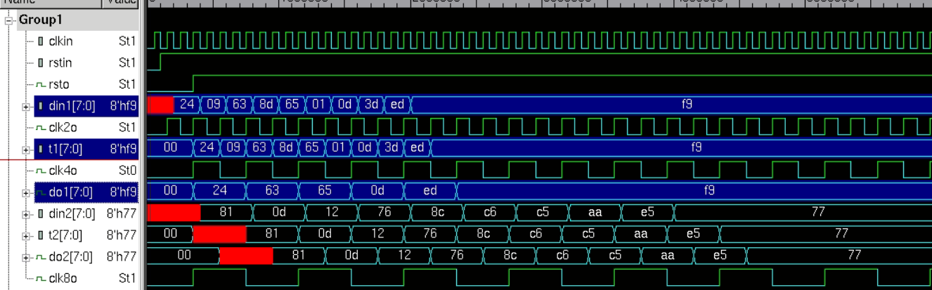
the design is cdc test setup din1-do1 is fast to slow cdc issue, do1 misses the one sample after each sample, din1 = 24 09 63 8d , do1=24 63 65 … like wise,if you not consider as cdc issue,then this circuit is perfectly multi-rate DSP down sampler by 1,, where as din2 – do2 is slow to fast cdc signal as from wf it not having any data loss.
By DVE tool , command by
vcs clk_rst_unit1.v cdc_test2.v tb.v +v2k -o simv -LDFLAGS -Wl,--no-as-needed -debug_all

the same data wave pattern as expected, din1 = 24 09 63 8d , do1=24 63 65 … like wise
for synthesis DC tool used and gscl45nm.v and saed90nm.v tech lib are used, tcl script is attached here for ref.
#/**************************************************
#/* Compile Script for Synopsys                    */
#/*                                                */
#/* dc_shell-t -f compile_dc.tcl                   */
#/*                                                */
#/* OSU FreePDK 45nm                               */
#/**************************************************/
file mkdir ../results/dc45
#/* All verilog files, separated by spaces         */

set fileFormat verilog              ;# verilog or VHDL
#set fileFormat VHDL              ;# verilog or VHDL

set my_hdl_files [list  ../code/clk_rst_unit1.v ../code/cdc_test2.v ]


#/* Top-level Module                               */
set my_toplevel cdc_test2

#/* The name of the clock pin. If no clock-pin     */
#/* exists, pick anything                          */
set my_clock_pin clkin
#create_clock -period 40 -waveform {0 20} -name clk

#/* Target frequency in MHz for optimization       */
set my_clk_freq_MHz 50

#/* Delay of input signals (Clock-to-Q, Package etc.)  */
set my_input_delay_ns 0.1

#/* Reserved time for output signals (Holdtime etc.)   */
set my_output_delay_ns 0.1


#/**************************************************/
#/* No modifications needed below                  */
#/**************************************************/
set OSU_FREEPDK /home/vlsi/libfortech/osu_freepdk/lib/files
set search_path [concat  $search_path $OSU_FREEPDK]
set alib_library_analysis_path $OSU_FREEPDK

set link_library [set target_library [concat  [list gscl45nm.db] [list dw_foundation.sldb]]]
set target_library "gscl45nm.db"
define_design_lib WORK -path ../WORK
set verilogout_show_unconnected_pins "true"
set_ultra_optimization true
set_ultra_optimization -force

#analyze -f vhdl    $my_hdl_files
analyze -f verilog $my_hdl_files

elaborate $my_toplevel

current_design $my_toplevel

link
uniquify

set my_period [expr 1000 / $my_clk_freq_MHz]

set find_clock [ find port [list $my_clock_pin] ]
if {  $find_clock != [list] } {
   set clk_name $my_clock_pin
   create_clock -period $my_period $clk_name
} else {
   set clk_name vclk
   create_clock -period $my_period -name $clk_name
}

set_driving_cell  -lib_cell INVX1  [all_inputs]
set_input_delay $my_input_delay_ns -clock $clk_name [remove_from_collection [all_inputs] $my_clock_pin]
set_output_delay $my_output_delay_ns -clock $clk_name [all_outputs]

compile -ungroup_all -map_effort medium

compile -incremental_mapping -map_effort medium

check_design
report_constraint -all_violators

set filename [format "%s%s"  $my_toplevel "s45.v"]
write -f verilog -output ../results/dc45/$filename
write -f verilog -output ../enc/$filename

set filename [format "%s%s"  $my_toplevel "s45.sdc"]
write_sdc ../results/dc45/$filename
write_sdc ../enc/$filename

#set filename [format "%s%s"  $my_toplevel "45.db"]
#write -f db -hier -output ../results/$filename

redirect ../results/dc45/timing45.rep { report_timing }
redirect ../results/dc45/cell45.rep { report_cell }
redirect ../results/dc45/power45.rep { report_power }

redirect  ../results/dc45/report_time45.txt {report_timing -path full -delay max -max_paths 1 -nworst 1}
redirect ../results/dc45/report_area45.txt {report_area}
redirect ../results/dc45/report_power45.txt {report_power}
exec cat ../results/dc45/report_area45.txt ../results/dc45/report_power45.txt ../results/dc45/report_time45.txt >  ../results/dc45/report_all45.txt
--------------
dc tcl script for 90nm tech
--------------
#/**************************************************
#/* Compile Script for Synopsys                    */
#/*                                                */
#/* dc_shell-t -f compile_dc.tcl                   */
#/*                                                */
#/* OSU FreePDK 45nm                               */
#/**************************************************/
file mkdir ../results/dc90
#/* All verilog files, separated by spaces         */
set fileFormat verilog              ;# verilog or VHDL
#set fileFormat VHDL              ;# verilog or VHDL

set my_hdl_files [list  ../code/clk_rst_unit1.v ../code/cdc_test2.v ]

#/* Top-level Module                               */
set my_toplevel cdc_test2

#/* The name of the clock pin. If no clock-pin     */
#/* exists, pick anything                          */
set my_clock_pin clkin
#create_clock -period 40 -waveform {0 20} -name clk

#/* Target frequency in MHz for optimization       */
set my_clk_freq_MHz 50

#/* Delay of input signals (Clock-to-Q, Package etc.)  */
set my_input_delay_ns 0.1

#/* Reserved time for output signals (Holdtime etc.)   */
set my_output_delay_ns 0.1


#/**************************************************/
#/* No modifications needed below                  */
#/**************************************************/

set saed90 /home/vlsi/libfortech/90nm/models
set  search_path     ${saed90}
set  link_library    ${saed90}/saed90nm_typ_ht.db
set  target_library  ${saed90}/saed90nm_typ_ht.db
set  symbol_library  ${saed90}/saed90nm.sdb
set  define_design_lib WORK -path ./WORK

alias h history
alias rc "report_constraint -all_violators"

#set OSU_FREEPDK /home/vlsi/libfortech/osu_freepdk/lib/files
#set search_path [concat  $search_path $OSU_FREEPDK]
#set alib_library_analysis_path $OSU_FREEPDK

#set link_library [set target_library [concat  [list gscl45nm.db] [list dw_foundation.sldb]]]
#set target_library "gscl45nm.db"
#define_design_lib WORK -path ../WORK
set verilogout_show_unconnected_pins "true"
set_ultra_optimization true
set_ultra_optimization -force

#analyze -f vhdl    $my_hdl_files
analyze -f verilog $my_hdl_files


elaborate $my_toplevel

current_design $my_toplevel

link
uniquify

set my_period [expr 1000 / $my_clk_freq_MHz]

set find_clock [ find port [list $my_clock_pin] ]
if {  $find_clock != [list] } {
   set clk_name $my_clock_pin
   create_clock -period $my_period $clk_name
} else {
   set clk_name vclk
   create_clock -period $my_period -name $clk_name
}


set_driving_cell  -lib_cell INVX1  [all_inputs]
set_input_delay $my_input_delay_ns -clock $clk_name [remove_from_collection [all_inputs] $my_clock_pin]
set_output_delay $my_output_delay_ns -clock $clk_name [all_outputs]

#create_clock -name "clk" -period 10 -waveform {"0" "5"} {"clk"}
#set_dont_touch_network find( clock, "clk")
set_fix_hold clkin
#set_operating_conditions "typical" -library "typical"
#set_wire_load_model -name "ForQA" -library "typical"
#set_wire_load_model -name tc8000000 -library saed90nm_typ_ht
set_wire_load_mode "segmented"
set_max_area 0


compile -ungroup_all -map_effort medium

compile -incremental_mapping -map_effort medium

check_design
report_constraint -all_violators

set filename [format "%s%s"  $my_toplevel "90.v"]
write -f verilog -output ../results/dc90/$filename
write -f verilog -output ../icc/$filename

set filename [format "%s%s"  $my_toplevel "90.sdc"]
write_sdc ../results/dc90/$filename
write_sdc ../icc/$filename


#set filename [format "%s%s"  $my_toplevel "45.db"]
#write -f db -hier -output ../results/$filename

redirect ../results/dc90/timing90.rep { report_timing }
redirect ../results/dc90/cell90.rep { report_cell }
redirect ../results/dc90/power90.rep { report_power }

redirect  ../results/dc90/report_time90.txt {report_timing -path full -delay max -max_paths 1 -nworst 1}
redirect ../results/dc90/report_area90.txt {report_area}
redirect ../results/dc90/report_power90.txt {report_power}
exec cat ../results/dc90/report_area90.txt ../results/dc90/report_power90.txt ../results/dc90/report_time90.txt >  ../results/dc90/report_all90.txt
-------------
from this script we get all reports, timing, area, power, GL netlist .sdc file as well. scr-sht of schematic 45nm and 90nm given below.


GL netlist names are cdc_test2s45.v and cdc_test290nm.v, for post simulation commands and wave form attached here for ref.
irun -access +rwc ./gscl45nm.v ./cdc_test2s45.v ./tb.v -gui -sv
irun -access +rwc ./saed90nm.v ./cdc_test290.v ./tb.v -gui -sv
//--------------
vcs  gscl45nm.v cdc_test2s45.v tb.v  +v2k -o simv -LDFLAGS -Wl,--no-as-needed  -debug_all
./simv -gui &
vcs  saed90nm.v cdc_test290.v tb.v  +v2k -o simv -LDFLAGS -Wl,--no-as-needed  -debug_all
./simv -gui &

above waveform is from irun tool, simvision , for 45nm as there is one sample data loss after each sample that issue is different, also there is meta-stability at cursor location do1 = 01h, we see this waveform again just keep it in memory[***].

dve tool wf 45nm same netlist, but here we see very strange result. here we have not get any data on both output buses, do1 and do2 as well.
for 90nm irun then dve tool result for post simulation


here function wise both wf from two diff tools matched, you can notice the glitches as transition on buses, still there one sample data loss at do1 due to cdc issue.
from[***] we can now focus/zoom little bit at courser location to see what actually happening there.


from waveform it is seen that on event of clk4o, data input is not stable 01,[and value 8D is stable], clk event happens so it lock the 01 at do1, which is not the correct value, even there is data loss of one sample after each sample read.
the codes and script will be available on request, any comment / feed back appreciated.